Home > SMT Assembly News
In Figure 1, the solder has failed to wet the lead termination but has wetted the through hole. In this case, the plating was found to be an issue as the brass pins had not been correctly plated with copper before tin lead plating. The copper plating is necessary to stop zinc migration affecting the tin/lead surface. A minimum of 0.002µm is necessary for long solderable life with a minimum of 0.005µm of tin/lead over the copper. The components are clearly at fault and this is not a problem associated with the soldering process.
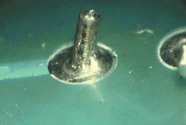
Figure 1: Here, the brass pins had not been plated with copper before tin lead plating.
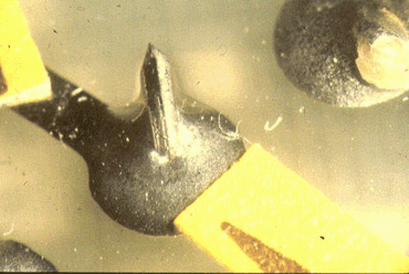
In Figure 2, the solder failed to wet the surface of the lead during wave contact even though there is evidence of satisfactory wetting on the pad. This problem was caused by marginal solderability of the leads and the age of the 10% solids flux being used in production. Replacing the flux and changing it regularly after forty hours of operation solved the problem. Flux in an open tank degrades; its performance changes even if the solids content remains the same. Using components and making sure they are rotated in stores also reduces the issue reoccurring. Component suppliers generally only guarantee their parts are solderable for a period of twelve months.
Poor solderability on tin/lead boards is uncommon if the correct thickness of tin/lead is applied to the pad surface. As a guide, a minimum thickness of 0.005µm should provide a solderable coating that will exceed a twelve month shelf life. It will most probably protect the surface in normal conditions for a couple of years and still be highly solderable.
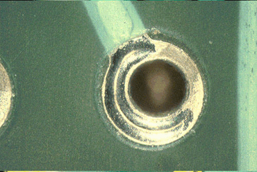
In the case of the sample shown in Figure 3 the tin/lead was less than 0.002µm on the surface of the board. It was also a plated finish that had not been reflowed during board manufacture, hence the shorter shelf life of the product. Only part of the through hole pad surface has wetted with solder; the outer and inner edge of the pad has failed to wet.
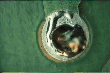
The pad in Figure 4 has failed to wet during soldering and is undoubtedly caused by the poor solderability of the pad surface. The reason for the poor wetting of the pad is a little more difficult to define. The solderability of the board should be tested as the surface would appear to have dewetted just after soldering which is likely to be related to the PCB.
Poor solderability of the pins can be caused by poor or thin plating or long storage times. Solderability of tin/lead pins normally is a function of the plating thickness or of the plating and the base materials. In the case of brass pins, the pin must first be plated with a 1-3µm layer of copper before the tin/lead is applied; otherwise zinc from the brass will affect the solderability very quickly.
Solderability is also related to thickness. If a coating of 0.005µm is present, it should provide in excess of one year's storage life. This coating thickness is relevant for any base materials. The example shown in Figure 5 is not a plating issue; it was caused by the printed board resin on the corner of the pins. If you look carefully you can see that only the corners of the pins has failed to wet. During pin insertion, the four corners of the pin have made an interference fit with the single-sided board, causing resin to smear along the corners.
When looking at any defects, don't jump to conclusions;, look at a number of defects using 10x magnification and just take a few minutes to think about the whole process, not just soldering.
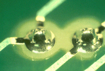
Figure 6 clearly shows poor wetting on the surface of the component leads with satisfactory pad wetting on the PCB. The component should be tested for solderability using a wetting balance or the dip and inspect test. Either the components have been stored for too long a period of time or the tin/lead coating on the leads was too thin. As an example, a tin/lead coating of 5µm should provide a solderable life in excess of one year.
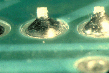
At first glance, the example in Figure 7 may be considered a skipped joint, but close examination shows it to be a solderability problem with the printed board coating. The gold surface coating is not wettable and needs to be discussed with the PCB manufacturer. It is normally caused by an out of balance electroless gold bath.

Incomplete wetting or poor solder rise in a plated through hole will show up due to poor fluxing or pre-heat temperature. If both are satisfactory, it will be the surface coating of the board. The trend in the industry is to copper surface finishes, but care must be taken over their selection. Special assembly conditions should also apply to storage, washing boards, cure and reflow temperature.
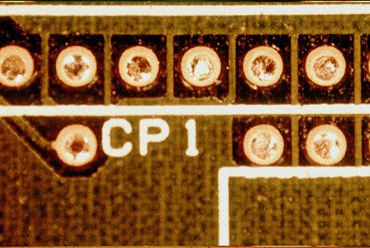
The solder joints on the IC in Figure 9 are satisfactory, with good fillets. The visual appearance of the leads are poor due to loss of the tin plating. Although the exposed leads will oxidise and are not likely to cause problems, the visual appearance will probably require the parts to be removed.
The loss of plating is due to poor initial plating probably during the preparation of the base lead frame prior to tin/lead coating. Loss of the coating is often seen at the lead to plastic interface due to mold flash contaminating the lead frame.
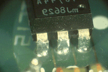
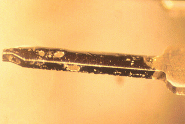
Poor solderability of the pins is not acceptable as these would form unreliable joints. The brass pins in Figure 10 have failed to wet with solder, in fact the tin plating has separated from the base material during soldering. The brass pins should have been plated with 1-2µm copper before tin/lead plating. What was astonishing was the supplier of these parts said that the components were perfectly solderable!
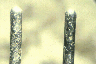
The solderability of the pin in Figure 11 was poor--after solder immersion the lead has failed to wet. The reason for the problem was thin tin/lead coating that resulted in poor wetting. A coating of 5µm should be used as a minimum to give a 12 month shelf life. Generally solderability problems are less likely with high activity fluxes and may increase as companies move to low residue low activity materials.
Keywords:
SMT Reflow Oven, Lead free Reflow Oven, Reflow Oven Manufacturer, LED reflow oven, PCB Reflow Oven, Nitrogen Reflow Oven, Dual Rail Reflow Oven, China Reflow Oven, wave soldering machine, Dual Rail Wave Soldering Machine, Nitrogen Wave Soldering Machine, Wave Soldering Machine Manufacturer.


Contact: Mr Tommy
Phone: +86 13691605420
Tel: +86 -755-85225569
Email: tommy@flason-smt.com
Add: 94#,Guangtian Road,Songgang Street,Bao an District Shenzhen China